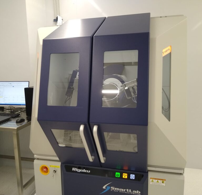
On Tuesday 14/12/2021, representatives of Politecnico and ST Microelectronics inaugurated the the cleanroom expansion for additional 210 m² that will host new equipment and joint research projects in Micro Electro-Mechanical Systems (MEMS) and motion control, as well as in power electronics and galvanic isolation.
With the core of ST’s global MEMS R&D operations located in Lombardy, close to Milan, the cooperation with PoliFab aims at setting up a center of excellence for studies and research on advanced materials for MEMS in the region.
The ongoing collaboration also encompasses investments in staff and programs, with ST supporting scholarships and the recruitment of professors and researchers, as well as financing joint research projects.
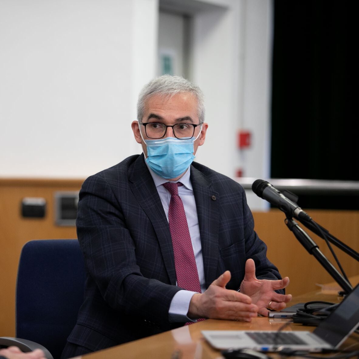
“We are pioneering a new model for “fast technology transfer” based on the realization of a joint research and innovation infrastructure where top-class semiconductor equipment, the very same used in a semiconductor fab, is made available to researchers and students,”
said Riccardo Bertacco, director of Polifab.
“Polifab 2.0 is a physical site where exciting scientific ideas can meet state-of-the-art semiconductor technology, thus speeding-up both fundamental research and its technology transfer.”

“Today’s event marks a significant milestone in building an Italy-unique, world-class semiconductor innovation hub that can contribute to ST’s R&D efforts in multiple areas including MEMS and sensors, one of the most promising technologies that enable digital transformation and the Internet of Things,” said Anton Hofmeister, Group Vice President and General Manager, R&D and Strategy for the Analog and MEMS Sub-Groups, STMicroelectronics.
“The successful collaboration with Politecnico is part of our global innovation strategy to foster high-caliber talent and facilitate industry-academia joint research programs as key elements of success in the global semiconductor market.”
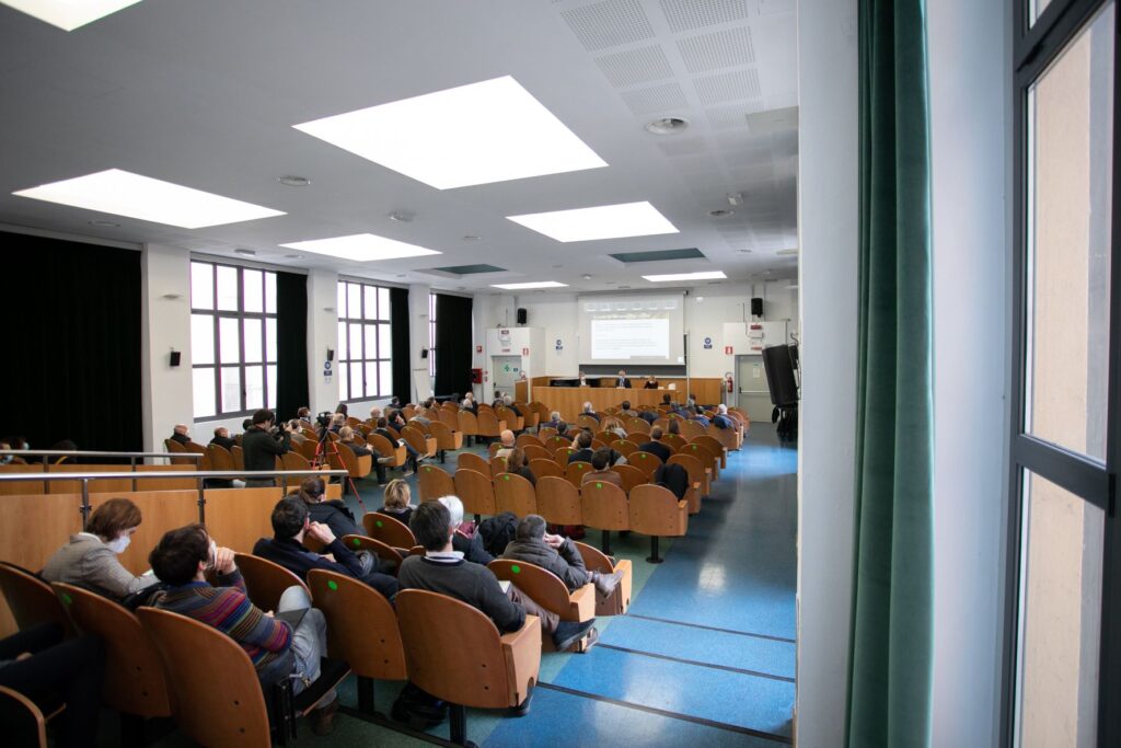
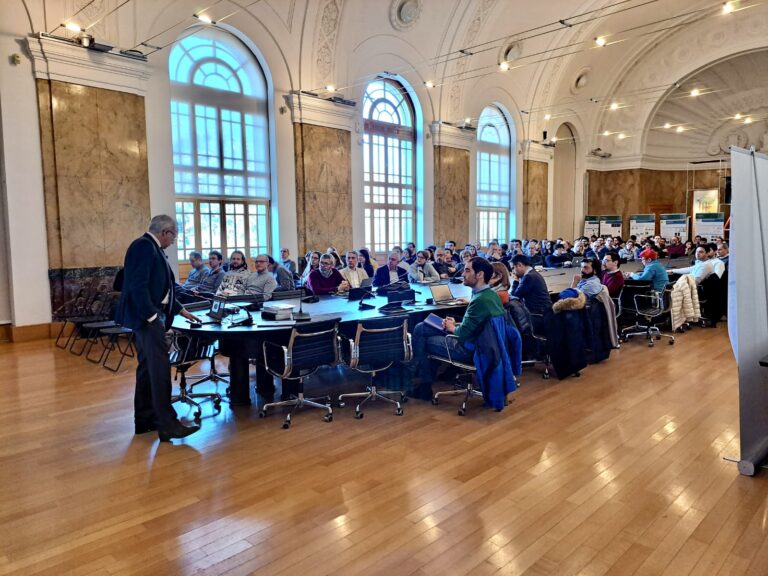
Inauguration Meeting in Auditorium 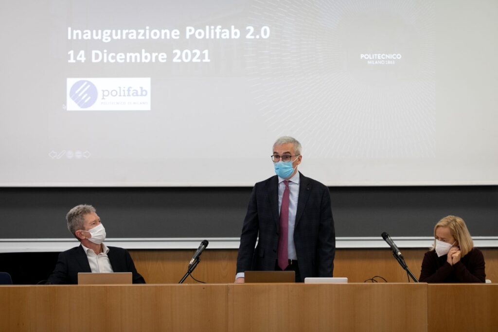
Anton Hofmeister, Riccardo Bertacco, Donatella Sciuto 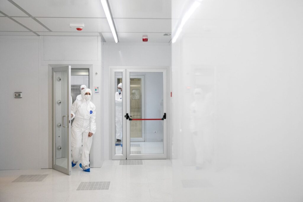
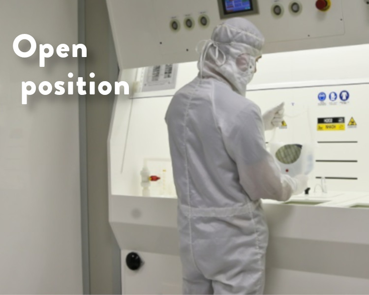
Entrance of the new cleanroom area
