LASSE (LAyered Structures for Spin Electronics)
Details
Description:
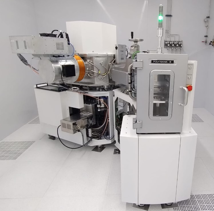
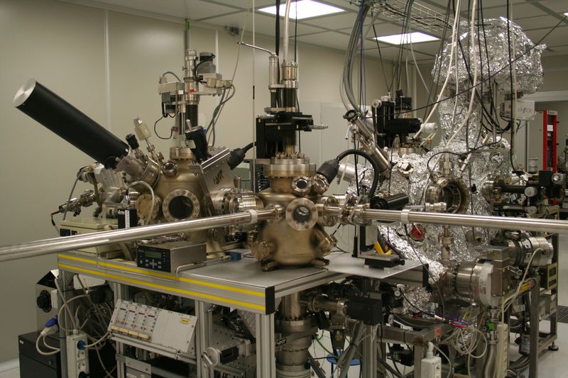
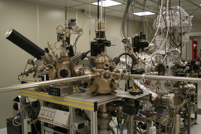
The LASSE (Layered Artificial Structures for Spin Electronics) cluster tool is a multi-chamber system, working in high vacuum conditions (pressure lower than 10-8 mbar), focused on the growth and characterization of films and heterostructures for spin electronics made by oxides (ferro-, ferri- and antiferro-magnetics, ferro-electrics, half metallic), 3d metals and semiconductors. The available in vacuum deposition techniques are pulsed-laser deposition (PLD) and molecular-beam epitaxy (MBE). Surface preparation can be performed in ultra-high vacuum conditions (pressure lower than 10-9 mbar) by thermal annealing and ion sputtering. Analysis and characterization of surfaces and interfaces can be performed in situ by means of electron spectroscopies, also with spin resolution, and diffraction techniques: x-ray and ultraviolet photoemission (XPS, UPS), spin-polarized inverse photoemission (SPIPE), low and high energy electron diffraction (LEED, RHEED), x-ray photoelectron diffraction (XPD). Moreover, magneto-optical Kerr effect (MOKE) allows for measuring in situ the magnetic properties of the sample. In addition, LASSE is equipped with a load-lock chamber for transferring samples, maintained in ultra-high vacuum conditions, to synchrotron radiation facilities (ESRF, ELETTRA-Trieste).
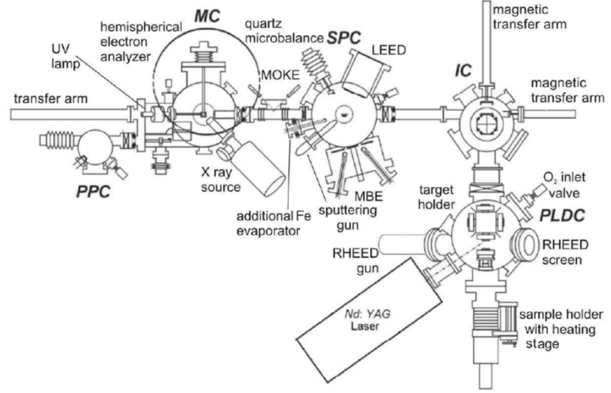
Schematic of the LASSE cluster tool
Working principle
LASSE is equipped by different techniques for thin films growth and characterization. A load lock chamber (IC) is employed for fast insertion and extraction of the sample into the cluster tool. The chamber can be pumped down from atmosphere to 10-7 mbar in few minutes for sample insertion, and vented in nitrogen in few seconds for sample extraction. A network of sample holders and magnetic and mechanic transfer-arms allows from moving the sample in the other chambers. PLD deposition is performed in the Pulsed-Laser Deposition chamber (PLDC), with base pressure lower than 5´10-9 mbar, equipped with a Reflection High Energy Electron Diffraction (RHEED) apparatus for real-time monitoring of the growth. RHEED employs a beam of high-energy (30-50 keV) electrons which strike the sample at a very small angle relative to the sample surface. Incident electrons diffract from atoms at the surface of the sample, and a small fraction of the diffracted electrons interferes constructively at specific angles and form regular patterns on the detector. The electrons interfere according to the position of atoms on the sample surface, so the diffraction pattern at the detector depends on the atomic structure/quality of the sample surface.
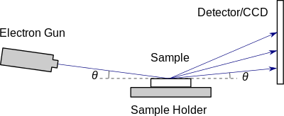
Schematics of the RHEED
Pulsed-Laser Deposition (PLD) is a technique based on the laser ablation of a target (i.e. the material to be deposited), which forms a plasma plume that is re-deposited on the surface of a substrate. PLD allows for transfer of even complex stoichiometries (e.g., complex oxides such as La0.7Sr0.3MnO3 and BaTiO3), in vacuum or oxygen pressure conditions.
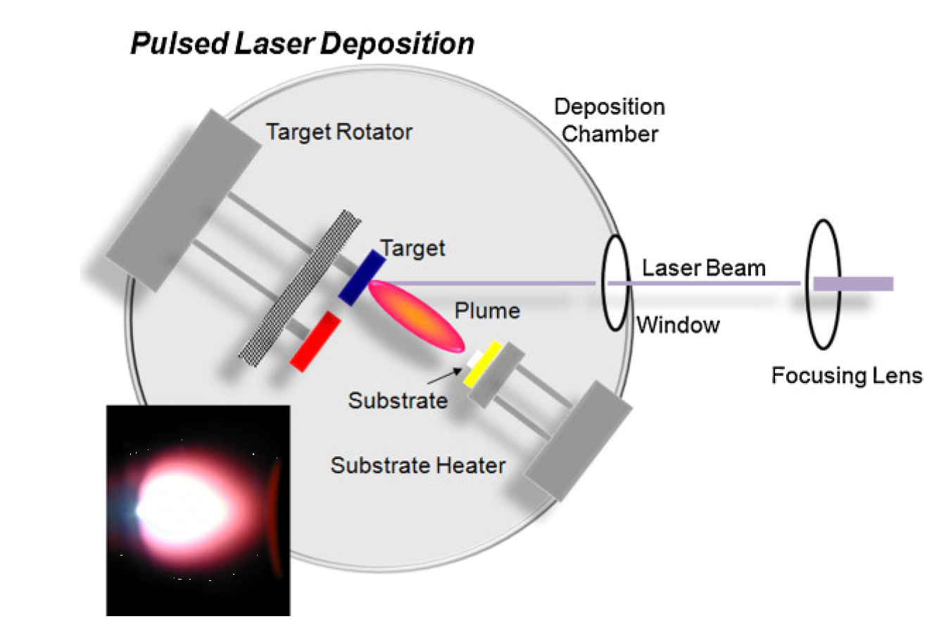
Schematics of the PLD deposition process
MBE is performed in the Sample Preparation Chamber (SPC) in ultra-high vacuum conditions (base pressure lower than 10-9 mbar). The chamber is also equipped with (i) a sputtering gun for sample cleaning, (ii) a dispenser of molecular oxygen for controlled oxidation processes, (iii) a thickness monitor to measure deposition rates and (iv) a Low Energy Electron Diffraction (LEED) apparatus.
Molecular Beam Epitaxy consists in heating by electron bombardment a material in form of a rod (such as Fe, Co, Ni, Au, Ag, Cr, Pd, Pt) or contained in a crucible (such as MgO, Ba, Sr, organic compounds). The peculiarity of MBE is the low deposition rate (down to about 0.1 nanometer per minute), allowing for epitaxial growth of the material on a suitable substrate.
LEED is a technique for the determination of the surface structure of single-crystalline materials by bombardment with a collimated beam of low energy electrons (20–200 eV) and observation of diffracted electrons as spots on a fluorescent screen.
Electron spectroscopy characterizations are done in the Measurement Chamber (MC) in ultra-high vacuum conditions (base pressure lower than 10-9 mbar).
In photoelectron spectroscopy techniques, a photon beam impinges on the surface of a sample and produces photo-ionization of the material. Photoelectrons escaping the sample are collected and counted by an electron analyzer as a function of their kinetic energy and/or emission angle. Depending on the photon energies, several information can be obtained. XPS (x-ray photoemission spectroscopy) gives access to core levels binding energies, leading to information on stoichiometry, chemical bindings (e.g. oxidized states) and surface and interface quality (sharpness, interdiffusion, etc.). UPS (ultraviolet photoemission spectroscopy) give access to the valence band density of states (up to few eV below the Fermi level). XPD (X-ray Photoelectron Diffraction) consists in XPS performed as a function of the emission angle of photoelectrons from the sample surface, and exploits diffraction effects between the photoelectrons inside the material. In addition to XPS features, this technique gives access to the chemically-resolved crystal structure of the sample. XPS, UPS and XPD are surface sensitive techniques, sensible to the first 2-5 nanometers from the sample surface.
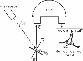
Schematics of X-ray Photoemission Spectroscopy, showing the acquisition of an iron core level (Fe 2p)
Inverse Photoemission Electron Spectrosocpy (IPES) is used to probe empty states of a material. An electron beam is produced illuminating a GaAs photocatode in the Photocatode Preparation Chamber (PPC) and focussing electrons using an electron gun. The beam reaches the sample surface and induces radiative transitions. A photodetector, composed by an energy band-pass filter, a photocatode converting photons into electrons, and an electron counter, measures the photon number as a function of the beam energy and, in the spin resolved version of the technique, of their spin. The spin resolved density of state of the conduction band (up to 23 eV above the Fermi level) can be measured, with a surface sensitivity of about 1 nanometer. In order to probe the magnetic properties of the sample, Magneto-Optical Kerr Effect (MOKE) is also available in MC. This technique is based on the reflection of a linearly polarized beam (visible or near infrared) from the surface of a magnetized sample. The magnetization vector affects the off-diagonal elements of the optical reflection matrix, leading to an elliptical polarization of the reflected beam. The analysis of such beam gives access to fundamental magnetic properties of the sample, such as the coercive field and the magnetization curve shape.
Specifications
Samples dimension: maximum size of about 10×10 mm2 PLDC: The laser employed for Pulsed Laser Deposition (PLD) is a Continuum Powerlite Precision II 8000 quadrupled Q-Switched Nd:YAG laser (266 nm), providing pulses 7 ns long at 2-10 Hz frequency with a fluence of 5.6 J/cm2. The sample holder can be rotated in front of the target and heated up to 920 K in oxygen atmosphere (up to 103 mbar), for pre- or post-annealing and during deposition. Targets are placed on a rotary stage, that can fit up to 4 different materials at the same time (e.g., Al, La0.7Sr0.3MnO3, SrTiO3, BaTiO3). The Reflection High Energy Electron Diffraction (RHEED) apparatus is a TorrRHEED, STAIB Instruments, equipped with a double differential pumping stage for working in oxygen pressure up to 100 mTorr (i.e. during PLD deposition), with electron energies up to 50 keV. SPC: The base pressure of the chamber is between 10-10 and 10-9 mbar (ultra-high vacuum, UHV). Molecular Beam Epitaxy (MBE) deposition is performed in UHV conditions employing 7 Knudsen cells, that can be operated separately or in a pair (e.g. for depositing alloys such as FeMn and NiFe). Materials currently deposited are Fe, Co, Ni, Au, Ag, Cr, Pd, Pt, Mn, MgO. Typical deposition rates are on the order of 0.1-1 nanometer per minute. The deposition rate is measured by a quartz microbalance (thickness monitor). The sample is mounted on a holder that can be heated up to 1000 K, for pre- and post-annealing processes or during deposition. A motorized shutter in front of the holder allows for deposition of samples with stepped or wedged structures. Sample cleaning before deposition can be performed by thermal annealing (up to 1000 K) and ion bombardment, employing a beam of Ar-ions accelerated by high voltage (from 500 V to 2 kV) and focused on the sample. A dispenser of molecular oxygen is present in order to perform controlled oxidation processes. The Low Energy Electron Apparatus (LEED) apparatus works in UHV conditions; the energy of the electrons is in the range 0-200 eV. MC: Two kind of photon sources for electron spectroscopy are available:
- x-ray source (from VSW) emitting photons with energies 1253.6 eV (Mg-Ka) and 1486.6 eV (Al-Ka);
- ultraviolet source (UVS 10/35 from SPECS) emitting photons with energies 21.2 eV (He-I) and 40.8 eV (He-II)
The electron analyzer is an Hemisperical Energy Analyzer (HEA) Phoibos 100/150 from SPECS with 9 channeltrons, with energy resolution down to 0.8 eV and spatial resolution down to 100 µm, depending on the operation modes. The Inverse Photoemission Detector employs a GaAs electron source with negative electron affinity (NEA), producing an electron beam with kinetic energy ranging from 0 fo 23 eV and a spin polarization of ±0.5. The energy resolution of the detector is 0.75 eV. The Magneto-Optical Kerr apparatus employs a red laser (635 nm, 5 mW) to illuminate the sample. A couple of coils allows magnetizing the sample in two perpendicular directions, with DC fields up to 10 mT and pulsed fields up to 300mT. The sample is mounted on a holder that can be cooled down to 120 K and heated up to 550 K. A Faraday Cup and a Tantalum reference sample are mounted in proximity of the sample position for calibration of the electron beam position and of the energy references, respectively.
Material
Software: CasaXPS software for XPS/UPS data analysis References:
- Description of the LASSE cluster tool
- Specifications of the Electron Analyser Phoibos 150
- Description of the Inverse Photoemission Detector

