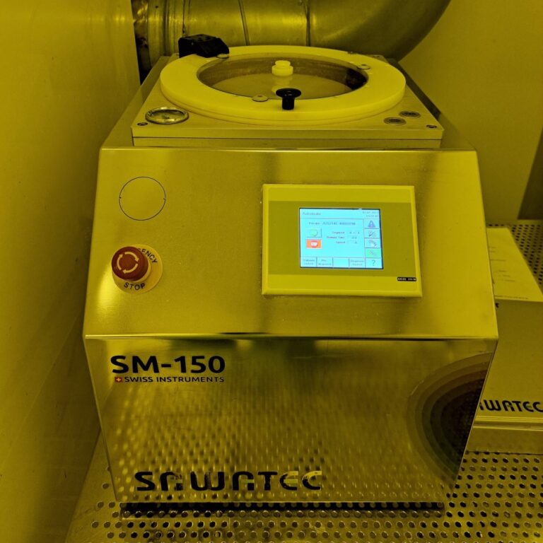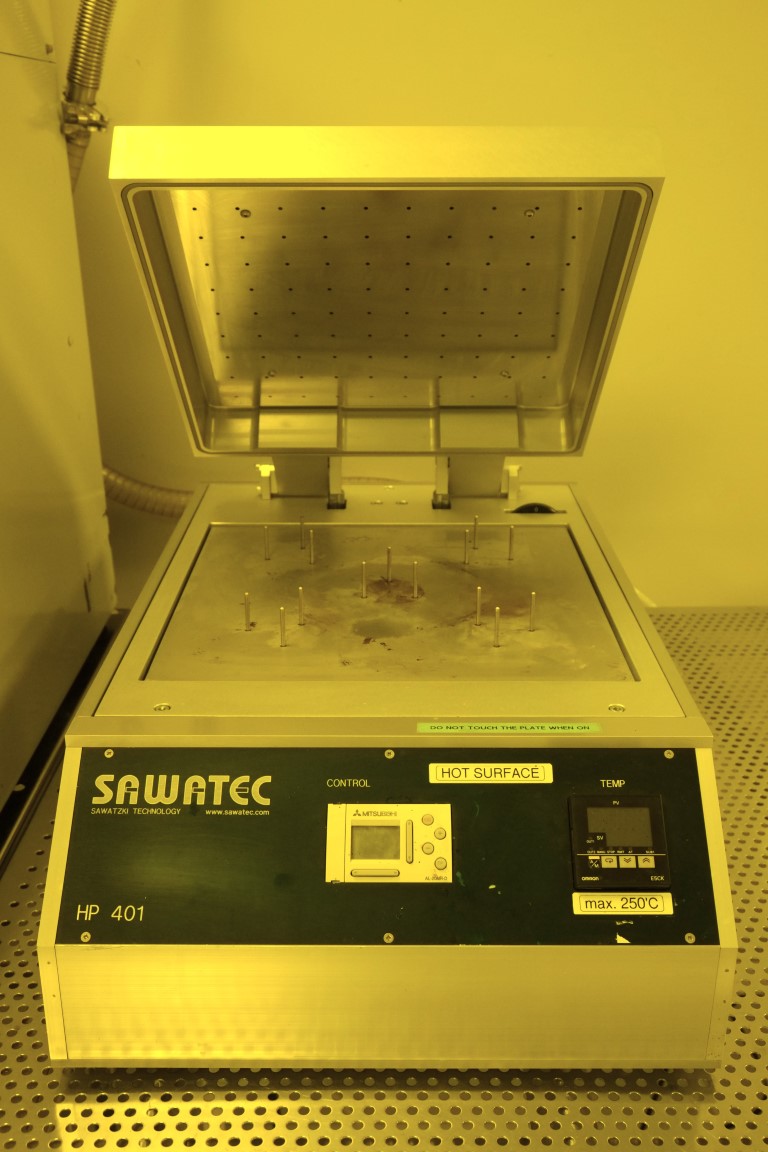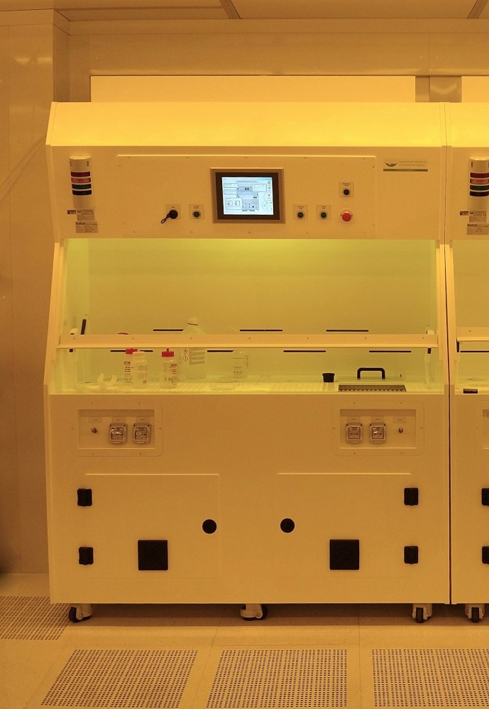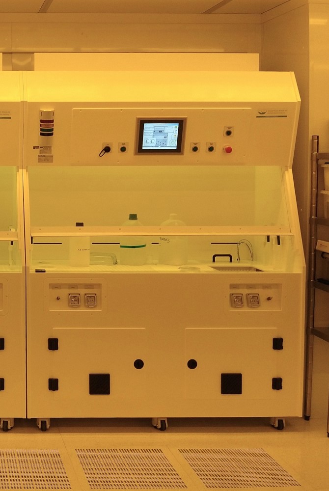
Developer Module – SAWATEC SMD-200
Details

Description
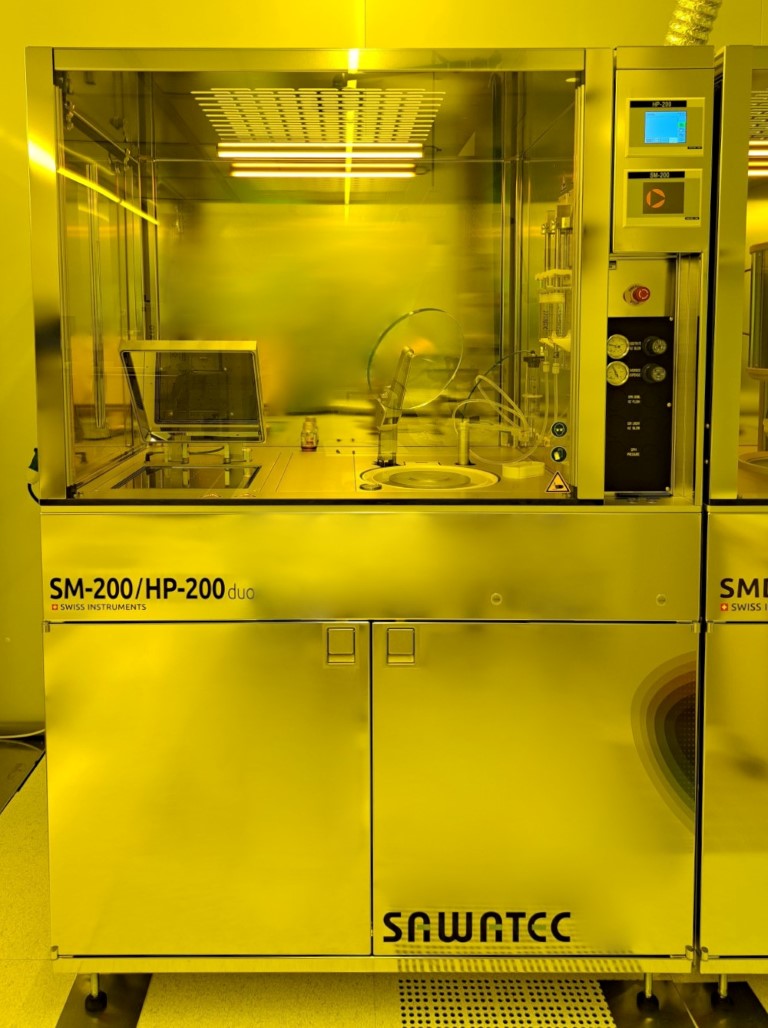
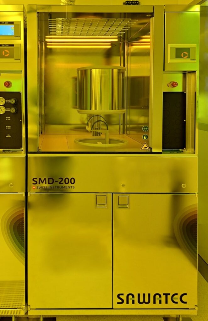
The SAWATEC SMD-200 developer handles cleaning and development of photoresist-coated substrates after exposure.
Development of the exposed photoresist is one of the most critical steps in photolithography, so special care must be taken when selecting the development process and its parameters (temperature, development time, etc.).
The SAWATEC developers can be used for puddle or spray development: the choice of the optimum process is based on application-technical and economic criteria. The advantage of the spray development is that very small fine structures can be released. The benefit of the puddle method is that significantly less developer solution is needed and better results are achieved when the substrate has deeper structures.
The exposed areas are continuously sprayed with fresh developing agent to prevent the developer from saturating.
The SMD-200 is designed to clean and to develop wafers up to 8” (200mm) or substrates up to 6”x6” (150 x 150mm). The process chamber works up to Ø 212mm.
Features
- Up to 50 programs with 24 segments each can be programmed
- Process parameters: speed, acceleration, process time, speed of the spray arm, developing spray time
- Electrical driven spray arm, with dynamic or static function
- Developer line and media tank (2 litre) for one developer included
- Nozzle for DI-water-rinse and N2 drying on the spray arm
- Nozzles in the process bowl for the backside rinse
- Control elements for dosing of the compressed air and vacuum
- Rotational direction can be selected (CW, CCW)
- Manual loading and unloading of the substrates
- Mechanical substrate fixation
Specifications
- Speed range: 0 to 3’000 rpm +/-1 rpm1
- Speed acceleration: 0 to 3’000 rpm in 0.3 seconds1
- Process time up to 2376 seconds
- Developer spray time 99 seconds/segment
- Speed of the spray arm 10 to 100 mm/second
- Rinse and N2 drying 99 seconds/segment
- Heatable process hood up to 50 °C
- Spray nozzle made of PEEK, 0.8 mm
1 Slower speed and acceleration for the process recommended

